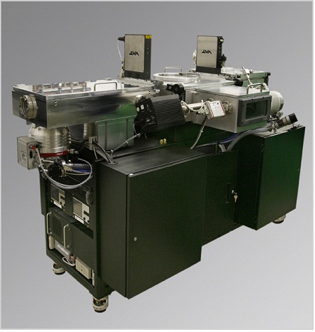
| Features:
7X improvement of thickness uniformity per single pass
20X ultimate thickness uniformity improvement
Throughput of up to 8 wafers per hour
Close to Zero minimum thickness loss if needed (patent pending)
Film thickness distribution adjustment to +/- 4A
Surface Roughness Improvement
Advantages:
Simple and robust transfer mechanism
DC based Ion Source - no filaments, no grids, simple maintenance
Millisecond response time
Zero minimum etch rate - does not require extra material deposition, and results in no degradation of the device
Thickness adjustment - of any Conductive and Non-conductive films
Cluster Tool combines Trimming Module and PVD Module for robust and economically advantageous approach to high scale manufacturing of FBAR/SAW devices
|